
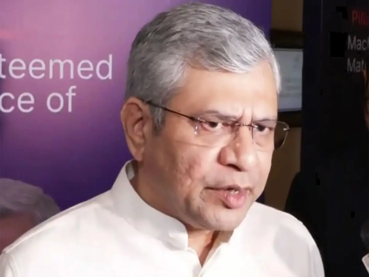
India is focused on becoming the AI application capital of the world, Union Minister Ashwini Vaishnaw said. He launched the Semicon 2.0 Web Application Portal to attract serious semiconductor players. The government also started work on indigenous graphics processing unit chips to boost the local electronics and manufacturing ecosystem further.
Synopsis
India is on a mission to become the global hub for artificial intelligence applications while also enhancing its semiconductor industry. With the launch of the Semicon 2.0 Web Application Portal, only well-prepared semiconductor enterprises will have their applications considered. The government is actively working on a strategy to produce indigenous graphics processing unit chips, alongside other crucial electronic components such as battery cells and copper foils.
Listen to this article in summarized format
India is focused on becoming the artificial intelligence (AI) "application capital" of the world, Union Electronics and Information Technology Minister Ashwini Vaishnaw said.
Speaking to media on the sidelines of the launch of the Semicon 2.0 Web Application Portal, Vaishnaw said the global AI industry is witnessing significant turbulence and rapid changes, with further developments expected as the technology continues to evolve.
"We in India are very focused on making India the application capital of the world," he said, adding that the industry's focus is on leveraging AI models across enterprises and transforming sectors such as agriculture, healthcare and education.
"All those applications, that is where a huge focus of our industry is, and they are progressing very well on this," he added.
Commenting on the launch of the Semicon 2.0 Web Application Portal, Vaishnaw said the platform has been designed to accept only complete applications, ensuring participation from serious players in the semiconductor industry.
"A special focus has been placed on preparing this portal that portals should accept only those applications which are complete in all respect," he said, adding, "The purpose of this is that only the extremely serious players should participate in this."
"There is no place for frivolous applicants," he stressed.
Apart from this, the Minister said the roadmap for developing an indigenous graphics processing unit (GPU) chip "is getting finalised."
Speaking at the launch event, Vaishnaw said the government would begin accepting applications under pillars two, three and four of the semiconductor programme, marking another step towards strengthening India's electronics and semiconductor manufacturing ecosystem.
"A lot of design expertise is getting built up. Lots of new things are coming... lots of new things are coming, and from today onwards, we'll start receiving applications for pillars two, three and four," he said, adding that "50% of the units approved are SMEs or MSMEs."
The Minister also highlighted India's growing capabilities in manufacturing critical electronic components and materials, including battery cells, copper foils and copper-clad laminates used in printed circuit boards (PCBs).
"Today we are making the entire battery cell. We are making copper foils. We are making copper-clad laminates for PCBs. In a sense, throughout that value chain, we are going deep with each program, with each approval," he added.